Experimental Measures of the Threshold Voltage and the Conductance Parameter of an NMOS-CD4007 Transistor
Introduction
Conventionally in our laboratory, we often measure the threshold voltage  by using a digital voltmeter (which has a high impedance) in series with a power supply and an NMOS (with gate tied to drain). The threshold voltage would be the supply voltage minus the reading from the voltmeter. However, different voltmeters gave different results (although the NMOS was the same). We then decided to derive the threshold voltage and conductance parameter by using curve fitting from measurements of drain current and gate-source voltage. Finally, we present two results with the channel-length modulation parameters: (1) neglected and (2) included.
Methodology
Data Acquisition
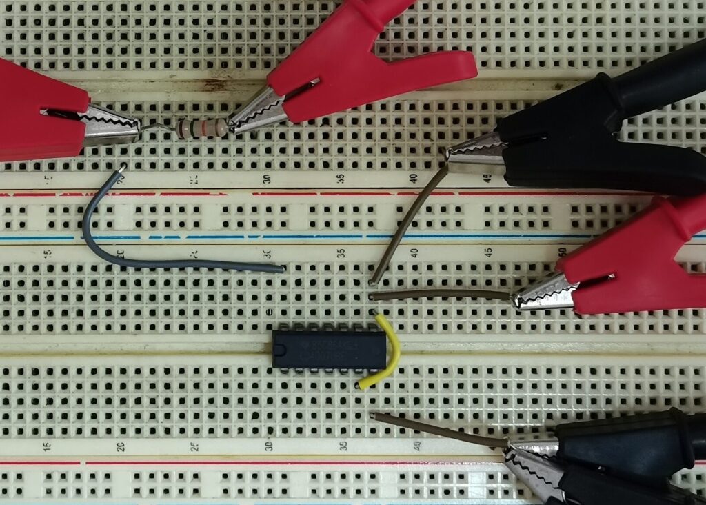
From Figure 1, an adjustable voltage source  , along with an arbitrary resistor
  , are used to supply the drain current
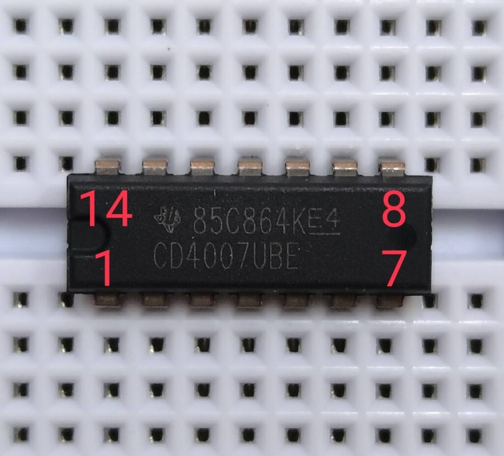
  into the MOSFET (CD4007, shown in Figure 2: gate at pin 6, source at pin 7 and drain at pin 8). Refer to Figure 3 for the breadboard connections. Adjust and to measure different and
  . The measurements were taken simultaneously using two multimeters shown as Figure 4.

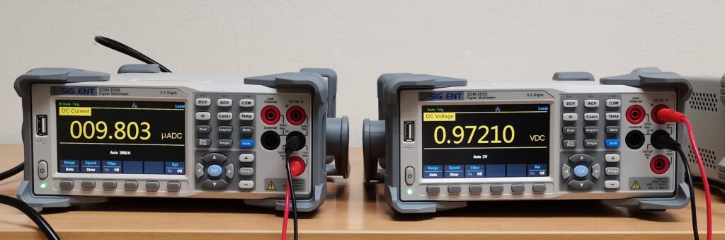 , right: a voltmeter to measure ).
Solving for Threshold Voltage and Conductance Parameter
Start with the drain current equation:
 .
.
Since the channel-length modulation parameter  could be neglected, we will divide our results into two cases: (1) assuming
  and (2)
  . For the first case (), the equation would be
 .
.
For the second case (), along with  , the equation would be
 .
.
After we formulate the problem into an equation, we then use a tool called Desmos to do curve fitting to find and  . Alternatively, one may use nonlinear optimization techniques such as rearranging the equation then minimize the residue or iterative search technique.
We will use the data with  to ensure that the NMOS is conducting.
Results
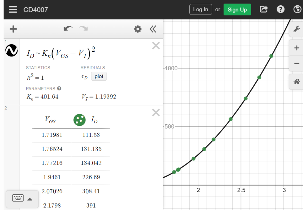
Neglecting the Channel-Length Modulation Parameter
We got  and
and  . The results can be viewed below (Figure 5) or at this interactive link.
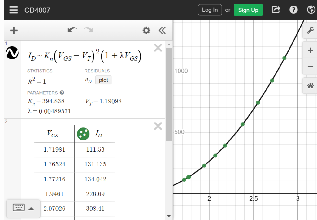
Including the Channel-Length Modulation Parameter
We got  ,
,  and
and  . The results can be viewed below (Figure 6) or at this interactive link.
Conclusions
This report measures threshold voltage and conduction parameter of an NMOS in a CD4007 Transistor package using curve-fitting technique. To improve the results in other regions, different drain voltages and source-body voltages may be explored in the future.
Acknowledgment
The author would like to thank Banlue Srisuchinwong for his devoted guidance and advices.